In the previous Verilog tutorial, we designed and simulated all seven basic logic gates (including, AND, OR, NOT, NAND, NOR, XOR, and XNOR) in Verilog. (If you haven’t been following this VHDL tutorial series step by step, it’s recommended to start here, and review the previous tutorials before continuing.)
In this tutorial, we’ll:
- Write a Verilog program to implement NAND, NOR, XOR, and XNOR gates using only AND, OR, and NOT gates.
- Simulate the program to design the digital circuits for these gates using the AND-OR-NOT implementation.
- Verify the output waveforms and compare them to the truth tables of these logic gates.
Let’s begin with the digital circuit for which we will write the Verilog program.
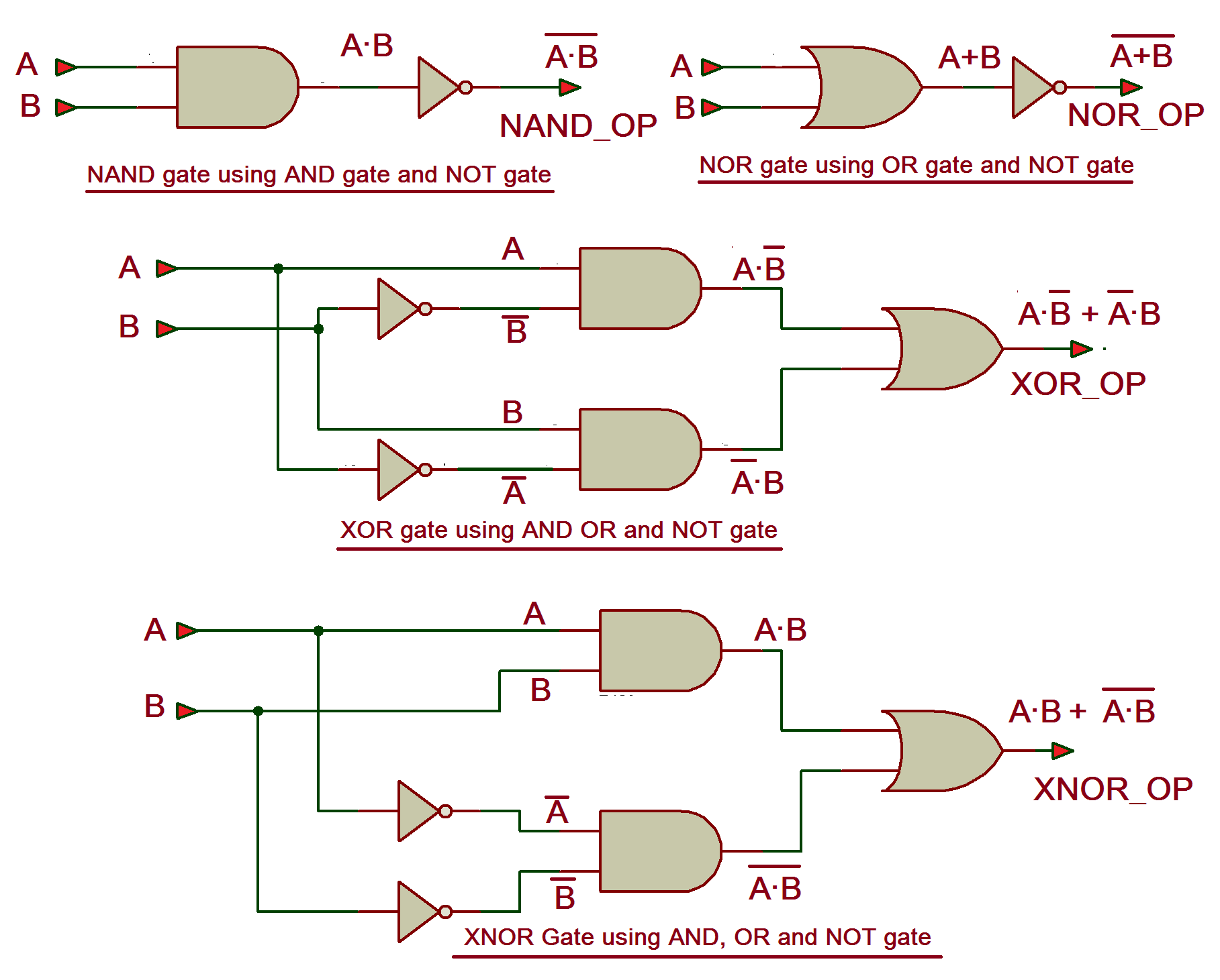
The truth tables
The truth table for the NAND gate using the AND-OR-NOT gate circuit:

The truth table for the NOR gate using the AND-OR-NOT gate:
 The truth table for the XOR gate using the AND-OR-NOT gate circuit:
 The truth table for the XNOR gate using the AND-OR-NOT gate circuit:

Now, let’s write a Verilog program, compile it, simulate it, and observe the output in the form of waveforms. Then, we’ll verify that the output waveforms match the corresponding truth table.
(For detailed steps on how to edit and compile the program, create a waveform file, simulate the program, and generate output waveforms, please refer to this tutorial.)
Verilog program
Gate-level modeling:
module AOI (a,b,y_nand,y_nor,y_xor,y_xnor);
input a,b;
output y_nand,y_nor,y_xor,y_xnor;
wire t1,t2,t3,t4,t5,t6,a_not,b_not;
and (t1, a, b);
not (y_nand, t1);
or (t2, a, b);
not (y_nor, t2);
not (a_not, a);
not (b_not, b);
and (t3, a, b_not);
and (t4, b, a_not);
or (y_xor, t3, t4);
and (t5, a, b);
and (t6, a_not, b_not);
or (y_xnor, t5, t6);
endmodule
Dataflow modeling:
module AOI (a,b,y_nand,y_nor,y_xor,y_xnor);
input a,b;
output y_nand,y_nor,y_xor,y_xnor;
assign y_nand = ~(a & b);
assign y_nor = ~(a | b);
assign y_xor = (a & ~b) | (~a & b);
assign y_xnor = (a & b) | (~a & ~b);
endmodule
Next, compile the program and create a waveform file including all the inputs and outputs. Simulate the project, and you should receive3 the following result.
Note: Write the program using one modeling style at a time, and then compile it. Afterward, you can modify the program to use another modeling style and recompile it. You can also experiment with a third modeling style, such as behavioral modeling (not covered here), and verify the results.
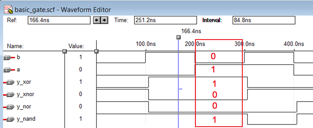
Compare the output waveforms with the truth table for the gates. For example, the highlighted case shows inputs “a = 1” and “b = 0.” You can verify the other three cases in a similar way.
This demonstrates how you can build NAND, NOR, XOR, and XNOR gates in Verilog using the AND-OR-NOT gates, verifying their outputs against the corresponding truth tables.
In the next tutorial, we’ll prove De Morgan’s Theorems by designing their digital circuits using Verilog programming.
You may also like:


Filed Under: Tutorials
Questions related to this article?
👉Ask and discuss on EDAboard.com and Electro-Tech-Online.com forums.
Tell Us What You Think!!
You must be logged in to post a comment.